The quest for new optoelectronic materials which are compatible with all-Si technology, thus enabling monolithic integration in light-emitting devices and photodetectors of conventional electronics, represents a great challenge of nowadays semiconductor research. One possibility consists in working with low-dimensional structures made of Si-compatible materials. Our group is thus concerned with the growth by molecular-beam epitaxy (MBE) of low-dimensional heterostructures such as quantum wells, wires and dots, which are based on type-IV semiconductors like Si and Ge with addition of C. We focus on the study of the physical properties which are crucial for the improvement of the performance for light emission of the obtained nanostructures by means of optical spectroscopies like Raman scattering, photoluminescence and spectral ellipsometry in combination with high-hydrostatic pressure techniques.
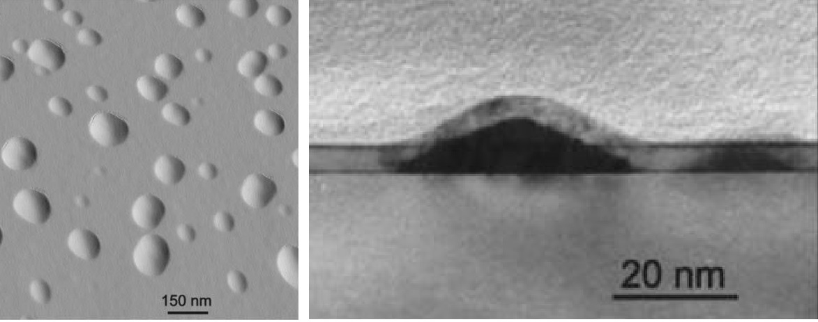
In particular, we make explicit use of the built-in stress components due to the large lattice mismatch between the different semiconductors like Si and Ge, to control the growth modus, switching between an epitaxial growth using strain-compensation techniques and a three-dimensional one in either Vollmer-Weber or Stranki-Krastanow mode for fabrication of SiGe quantum dots and in-plane nanowires. In this way, we might be able to tailor the electronic states in the obtained nanostructures to improve light emission or absorption efficiency.
The problem of attaining bright light emission from group IV semiconductors is of fundamental physical origin: both Si and Ge are indirect band-gap materials. As a consequence, the luminescence from group-IV materials is at least five orders of magnitude less intense than for their III-V counterparts. We aim, for instance, at tailoring the residual strain in novel micro-fabricated pure Ge or Ge-rich SiGe alloy layers, which when freed from the substrate should be able to concentrate large amounts of tensile strain to induce an indirect-to-direct gap crossover.
Another route towards attaining efficient light emitting materials fully compatible with CMOS technology concerns the use of amorphous Si nanoparticles (a-NPs) embedded in a non-stoichometric silicon oxide matrix. Our main finding is that the a-Si NPs exhibit intense, broadband emission in the visible, spectrally separable from the defect luminescence of the suboxide matrix. Apart from the brightness of the emitted light, the nanometer-sized a-Si inclusions present the technological advantage of needing very moderate annealing temperatures (450-700 C) for their production.
KEYWORDS: SiGe heterostructures; quantum wires and dots; optical, electronic & vibrational properties; spectroscopy; light emission.
Frequent collaborators: Dr. Jozef Novak (Bratislava); Dr. Riccardo Rurali (ICMAB); Prof. Axel Hoffmann (TU Berlin); Dr. Ana Ruiz (ICMM); Prof. Javier Rodríguez Viejo (UAB)
Contact: Mª Isabel Alonso (isabel@icmab.es), Alejandro Goñi (goni@icmab.es), Miquel Garriga (miquel@icmab.es) and Pablo Vaccaro (pvaccaro@icmab.es)