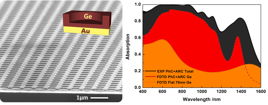
In our paper in Advanced Materials (P. Molet et al. 10.1002/adma.201705876), we greatly boost the absorption of thin layer of Ge (70nm) from 400nm until 1500nm. Furthermore, we do so by nanostructuring the semiconductor using nanoimprinting lithography, a technique compatible with mass production processes such as roll to roll.
We have provided the key design guidelines to tune the absorption profile of the ultrathin Ge metasurfaces and described the physical origin beneath each resonant mode sustained by the architecture. With these findings, we have shown strong broadband absorption (appealing to PV community) and NIR absorption peaks reaching 100% at the telecommunication windows (interesting to the photodetection field).
Link to the paper:
http://onlinelibrary.wiley.com/doi/10.1002/adma.201705876/full