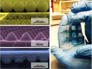
This research line focuses in three aspects:
- The investigation of the fundaments behind the enhanced light-matter interaction observed in devices that use wave optics components.
- The development of fabrication routes for large area and low cost photonic and plasmonic structures using techniques similar to those employed in industry, so they could be easily incorporated in technologies such as roll to roll.
- The fabrication and characterization of prototype solar cells, photodetectors and sensors based in photonic architectures, demonstrating improved performance without deterioration of other figures of merit in the device.
This research line relies on unconventional nanofabrication to produce photonic architectures with exciting optical properties easily incorporated into large area devices. We have the capabilities to design photonic nanostructures for each device type using current numerical simulation tools. We combine soft nanolithography, transfer printing and industry compatible fabrication approaches to integrate the architectures as part of the optoelectronic devices. Finally, we characterize optically and electrically the enhanced prototypes employing state of the art spectroscopic equipment.

KEYWORDS: Photonic crystals, plasmonics, nanoimprinting lithography, solar cells, thin films and SERS
Contact: Agustín Mihi (amihi@icmab.es)

